It looks like you're using an Ad Blocker.
Please white-list or disable AboveTopSecret.com in your ad-blocking tool.
Thank you.
Some features of ATS will be disabled while you continue to use an ad-blocker.

Print your own electrical circuits with modified inkjet
page: 19
share:
Hello ATS:
Here's an interesting little tidbit of technology for the electronics geeks of ATS:
Georgia Tech Develops Inkjet-Based Circuits at Fraction of Time and Cost
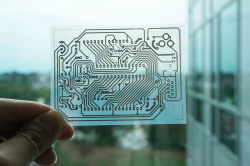
This could be very important for rapid prototyping of circuits. They use silver nanoparticle ink, and you can print on flexible transparent PET film, like in the picture, or on more rigid materials.
Electrical components can be adhered with silver adhesive compound. This might have helped me when I was wire-wrapping IC's on a breadboard 25 years ago.
Here's an interesting little tidbit of technology for the electronics geeks of ATS:
Georgia Tech Develops Inkjet-Based Circuits at Fraction of Time and Cost
Researchers from Georgia Tech, the University of Tokyo and Microsoft Research have developed a novel method to rapidly and cheaply make electrical circuits by printing them with commodity inkjet printers and off-the-shelf materials. For about $300 in equipment costs, anyone can produce working electrical circuits in the 60 seconds it takes to print them. - See more at: www.cc.gatech.edu...
This could be very important for rapid prototyping of circuits. They use silver nanoparticle ink, and you can print on flexible transparent PET film, like in the picture, or on more rigid materials.
Electrical components can be adhered with silver adhesive compound. This might have helped me when I was wire-wrapping IC's on a breadboard 25 years ago.
sounds good for prototyping at the moment but for more production especially multi layered boards where space is a virtue then it won't really have
much impact, but for proof of concept it sounds great
This is pretty neat, but I am wondering what implications this will have for various industries. Among the general population, I cannot imagine there
would be all that many people with the skill-set necessary as well as the need to use such a product/method. Then there are the companies who need to
print up boards. Those wishing to print up large volumes of such will probably have them produced in bulk somewhere else. I could see it helping the
smaller companies or individuals who don't need a large number of circuit boards, who can then print them up on demand. But like you said, prototyping
will be enhanced as well.
Overall, this technology will be beneficial in various ways, even if they are hard to see at the moment. Sort of like how it is with all technology. It really is cool as well. Good stuff.
Overall, this technology will be beneficial in various ways, even if they are hard to see at the moment. Sort of like how it is with all technology. It really is cool as well. Good stuff.
edit on 11/7/13 by JiggyPotamus because: (no reason given)
reply to post by InTheFlesh1980
Wondeful development and a new more ecological industrial scale method will likely be the outcome as well, makes a change from my days of dippin copper laminated boards into hydroflouric acid with hand drawn circuits which is though now machine printed still the way it is done but this is more efficiant on material and much more eco friendly, welcome to the new age of electronic inventors, be even better when discreet componants can be produced in 3d printers.
Wondeful development and a new more ecological industrial scale method will likely be the outcome as well, makes a change from my days of dippin copper laminated boards into hydroflouric acid with hand drawn circuits which is though now machine printed still the way it is done but this is more efficiant on material and much more eco friendly, welcome to the new age of electronic inventors, be even better when discreet componants can be produced in 3d printers.
Maxatoria
sounds good for prototyping at the moment but for more production especially multi layered boards where space is a virtue then it won't really have much impact, but for proof of concept it sounds great
For multi layered boards could you not simply print the layer on film and just stack them! I cannot see any reason that this would not work. I used to to do a lot of prototype boards and this would seem to be a godsend.
Great for prototypes as you mentioned!
How about 3D printing using this ink whenever you need a conductive layer. Anything that allows the little guy to make things is always great news.
P
InTheFlesh1980
This might have helped me when I was wire-wrapping IC's on a breadboard 25 years ago.
Tell me about it! This breathes new hope into my dream of making a Knight Rider dash for my Trans Am.
new topics
-
Where should Trump hold his next rally
2024 Elections: 1 hours ago -
Shocking Number of Voters are Open to Committing Election Fraud
US Political Madness: 2 hours ago -
Gov Kristi Noem Shot and Killed "Less Than Worthless Dog" and a 'Smelly Goat
2024 Elections: 3 hours ago -
Falkville Robot-Man
Aliens and UFOs: 3 hours ago -
James O’Keefe: I have evidence that exposes the CIA, and it’s on camera.
Whistle Blowers and Leaked Documents: 4 hours ago -
Australian PM says the quiet part out loud - "free speech is a threat to democratic dicourse"...?!
New World Order: 5 hours ago -
Ireland VS Globalists
Social Issues and Civil Unrest: 5 hours ago -
Biden "Happy To Debate Trump"
2024 Elections: 6 hours ago -
RAAF airbase in Roswell, New Mexico is on fire
Aliens and UFOs: 6 hours ago -
What is the white pill?
Philosophy and Metaphysics: 7 hours ago
top topics
-
A Warning to America: 25 Ways the US is Being Destroyed
New World Order: 16 hours ago, 21 flags -
James O’Keefe: I have evidence that exposes the CIA, and it’s on camera.
Whistle Blowers and Leaked Documents: 4 hours ago, 12 flags -
Blast from the past: ATS Review Podcast, 2006: With All Three Amigos
Member PODcasts: 8 hours ago, 11 flags -
Australian PM says the quiet part out loud - "free speech is a threat to democratic dicourse"...?!
New World Order: 5 hours ago, 10 flags -
Biden "Happy To Debate Trump"
2024 Elections: 6 hours ago, 10 flags -
Mike Pinder The Moody Blues R.I.P.
Music: 8 hours ago, 8 flags -
Ireland VS Globalists
Social Issues and Civil Unrest: 5 hours ago, 5 flags -
RAAF airbase in Roswell, New Mexico is on fire
Aliens and UFOs: 6 hours ago, 5 flags -
What is the white pill?
Philosophy and Metaphysics: 7 hours ago, 5 flags -
Putin, Russia and the Great Architects of the Universe
ATS Skunk Works: 11 hours ago, 4 flags
9