It looks like you're using an Ad Blocker.
Please white-list or disable AboveTopSecret.com in your ad-blocking tool.
Thank you.
Some features of ATS will be disabled while you continue to use an ad-blocker.

Will This Be The Future of Electronics?
page: 114
share:
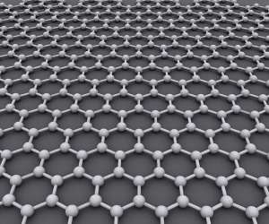
Future of Electronics: Single-Layer Molybdenite Transistors Trump both Silicon and Graphene
Just published over the weekend in the journal Nature Nanotechnology, a group from EPFL’s Laboratory of Nanoscale Electronics and Structures (LANES) are claiming that experiments and research carried out on the electrical properties of Molybdenite, a common and widely available material, have shown a remarkable improvement in the materials electrical characteristics when compared against both Silicon and Graphene.
As we know, Silicon is expensive and time consuming to engineer into electronics and chips, and while Graphene was looking like it may become Silicon's successor in electronics and transistor manufacture, it turns out to have a few limitations, which would make manufacturing devices problematic.
Molybdenite on the other hand, has been found to be not only perfect for taking over where Silicon will be phased out, but a sheet of Molybdenite just 0.65nm thick, can perform the same functions as a sheet of Silicon four times as thick, and do it in an area just 1/3 the size of conventional Silicon electronics.
It turns out to have ideal properties for electronics, chips, transistors and a slew of other applications is probably just waiting in the wings for this material, Solar energy generation/harvesting is probably just one of these areas yet to be explored by researchers.
The *real* plus point for Molybdenite electronics is from it's energy requirements.
A transistor (or CPU eventually) made from Molybdenite is estimated to consume just 1/100,000th the energy requirements as a similar transistor made from Silicon would use.
That's one, one hundred-thousandth of the energy of Silicon!
If this turns out to be in the ball park, i would reckon that devices, especially hand held units like phones and data tablets etc, would be able to be powered simply from the heat from your hands holding it...or by a tiny Solar strip on the side of the unit...1/100,000th remember!
The story itself does go on to state that it won't mean our electronic devices will consume 100,000X less energy than our Silicon devices currently consume (due to mechanical components, screens, drives etc still using substantial energy), but the individual electronic components themselves rather than the whole device would.
It's very early days still, but there are applications where this would be very useful now.
Space craft and probes should be able to made orders of magnitude smaller, and therefore last orders of magnitude longer...couple this with an electric Ion drive and we have a very long lasting power source for our probes.
If this stuff generates electricity at a similar ratio, and is fashioned into a Solar panel, think of what that would mean!
A solar panel just a few inches square, would in theory be able to power a home...Just shining a battery powered torch at the thing should generate enough energy during the night too.
What with cold fusion back on the menu and now this Molybdenite discovery, the future is so bright...we all may have to wear shades!
Here's a link to the story and a snippet or two of the story itself..enjoy.
www.popsci.com...
For one, molybdenite is a two-dimensional material, meaning it is less voluminous than three-dimensional silicon. Electrons can move around as freely in a 0.65-nanometer-thick sheet of molybdenite as they can in a 2-nanometer-thick layer of silicon, ostensibly requiring roughly one third the space to accomplish similar ends. It also possesses an ideal “gap” for turning transistors on and off, meaning a transistor with molybdenite’s 1.8 electron-volt gap could consume 100,000 times less energy than its silicon counterpart.
Further, molybdenite contains the necessary band gap needed to control semiconductors’ material properties. Electron-free spaces between these “band gaps” that allow certain electrons to leap across lend a greater level of control over a material’s electrical properties. Molybdenite has this gap. Graphene does not, making it less-than-ideal for transistor applications
Wow, this is crazy.
Molybdenite is used as a dry lubricant(bearings, aircraft engines, ski glide wax, ...).
The guys from Berkeley Lab are using titanium dioxide as a very efficient photocatalyst(www.abovetopsecret.com...).
What's next?
Molybdenite is used as a dry lubricant(bearings, aircraft engines, ski glide wax, ...).
The guys from Berkeley Lab are using titanium dioxide as a very efficient photocatalyst(www.abovetopsecret.com...).
What's next?
I guess Folks do not understand what this is all about, very nice advance in my opinion. It is also nice to find something in abundance as well,
usually when the next best thing comes out it is impossible to make like Graphene was in the beginning...where is my Molybdenite Core I7 already,
second gen comes out next month, lol.
First, this should greatly reduce the cost of chips and chipset, motherboards and anything else that makes parts with silicon.
Second, Graphene will be used in the future for transistors or anything power related since it has less resistance but everything else with this Molybdenite material will be smaller, cheaper, and then since this new material uses less electricity to power the circuit then some batteries issues will disappear.
I pulled some info on Molybdenite:
en.wikipedia.org...
And golly gee, look where we find the stuff:
“Important deposits include the disseminated porphyry molybdenum deposits at Questa, New Mexico and the Henderson and Climax mines in Colorado. Molybdenite also occurs in porphyry copper deposits of Arizona, Utah, and Mexico.”
I personally know the Climax mine well, my father worked there for years, and it has since slowed way down, and I believe it even closed for a few years. Glad to hear Leadville will boom again, and hopefully bring a lot of jobs back home to mining this stuff.
Star and flag!
Amazing research. Let's hope this heralds the dawn of cheaper, more efficient computers, processors, phones, tablets and cameras. Not to mention the many other applications this could be applied to.
I think the energy generation side of this is the most startling. Who wouldn't want a few square inches of solar panel on their roof to supply all their electricity needs?
reply to post by the.lights
It has to be said that the Solar panel thing is just me surmising, and didn't actually come from the research...but here's hoping.
It has to be said that the Solar panel thing is just me surmising, and didn't actually come from the research...but here's hoping.
A solar panel just a few inches square, would in theory be able to power a home...
Yeah, this won't work unfortunately. Solar power is about 150 to 300 W/m² on ground.
reply to post by moebius
It could work if you had a light condenser, in essense a magnifying glass, locater over the solar panel. By condensing the light from say a three foot diameter focal device, that would greatly enhance the amount of sunlight landing on the smaller solar panel. It is a lot cheaper making a plastic magnifying lens than it is to make a much larger solar panel.
Just a thought. You have made some good points. You obviously know a lot about this area of physics!
reply to post by Truth1000
You took the words right out of my mouth.
A sunlight concentrator, either a Fresnel lens affair or a parabolic trough/dish effort shining the concentrated light onto the panel should do it.
This very technology is being trialled in Israel at the moment with great success apparently, but using small, conventional Silicon panels approx six inches (or so) square...i was imagining what would happen if Molybdenite could generate 100,000X more than a Silicon panel would..even two or three times more would be great.
But yeah, i get that Solar is dependant on the amount of light hitting it and that as powerful as the sun is, it has a power per m2 limit.
If this material is as efficient as it looks to be, then i can imagine a scenario where artificial light with a greater light intensity than the sun itself was used as the source...think large, enclosed 'Bucky ball' type of thing.
The Bucky ball itself would be made of Hexagonal shaped Molybdenite panels, and the light source would be suspended in the centre. The light could be a microwave quartz sphere or even a dramatically cut down version of something like these:
The world's brightest torch:
technology.timesonline.co.uk...
Failing that, another idea would be the same 'Bucky ball' shaped sphere, only this time, the hex panels on the exterior could be made from hexagonal Fresnels, and the focus point, would be a small panel made of this new material (assuming it works for solar panels).
Light from any direction would be captured and focused by the lenses, i doubt we'd even need to track the sun.
Just throwing ideas about really...you never know, a highly placed engineer might read it and think about trying it out.
You took the words right out of my mouth.
A sunlight concentrator, either a Fresnel lens affair or a parabolic trough/dish effort shining the concentrated light onto the panel should do it.
This very technology is being trialled in Israel at the moment with great success apparently, but using small, conventional Silicon panels approx six inches (or so) square...i was imagining what would happen if Molybdenite could generate 100,000X more than a Silicon panel would..even two or three times more would be great.
But yeah, i get that Solar is dependant on the amount of light hitting it and that as powerful as the sun is, it has a power per m2 limit.
If this material is as efficient as it looks to be, then i can imagine a scenario where artificial light with a greater light intensity than the sun itself was used as the source...think large, enclosed 'Bucky ball' type of thing.
The Bucky ball itself would be made of Hexagonal shaped Molybdenite panels, and the light source would be suspended in the centre. The light could be a microwave quartz sphere or even a dramatically cut down version of something like these:
The world's brightest torch:
SCIENTISTS have created the world’s brightest light and will use it to look at molecules and atoms in more detail than before. The beam, made of synchronic light — created when electrons are fired in a vacuum along a circular tube at close to the speed of light — is almost 100 billion times brighter than the Sun and will be the light source of a £373million “giant microscope”, the Diamond project, being built in Didcot, Oxfordshire.
technology.timesonline.co.uk...
Failing that, another idea would be the same 'Bucky ball' shaped sphere, only this time, the hex panels on the exterior could be made from hexagonal Fresnels, and the focus point, would be a small panel made of this new material (assuming it works for solar panels).
Light from any direction would be captured and focused by the lenses, i doubt we'd even need to track the sun.
Just throwing ideas about really...you never know, a highly placed engineer might read it and think about trying it out.
Originally posted by moebius
Wow, this is crazy.
Molybdenite is used as a dry lubricant(bearings, aircraft engines, ski glide wax, ...).
The guys from Berkeley Lab are using titanium dioxide as a very efficient photocatalyst(www.abovetopsecret.com...).
What's next?
Cheers for the link moebius, really interesting time ahead i reckon.
Hadn't heard about this work with Titanium before...100X more hydrogen production than other catalysts?!!
Wow!
Think what just this one catalyst could do for energy production. This will make Hydrogen on demand systems much more promising. It's estimated that to drive a vehicle exclusively on H (or HHO), we'd need between 60 - 80 litres per minute (lpm).. People working on HHO (Hydroxy, Browns gas, etc) are already producing 10 - 20 lpm just using a couple of hundred watts..if we say we can produce just 1 lpm (we can make much more than that) using the catalysts we have now and 100 watts, if this catalysing technology comes to market, we could be looking at producing 100 lpm for the same energy input!
That is plenty to run a vehicle or home power generator.
Fun times ahead.
Cheers.
Originally posted by spikey
reply to post by Truth1000
A sunlight concentrator, either a Fresnel lens affair or a parabolic trough/dish effort shining the concentrated light onto the panel should do it.
You mean like the solar concentrator mentioned recently in several ATS threads? You know the one the size of a home satellite dish (it originally was a satellite dish) covered with 3,800 tiny mirrors. The one that melted or burned everything put in front of it. That's not going to also melt a solar panel?
Great science though. And my favorite part is it sounds like it isn't going to be one of those "in 10 years ..." deals. It can be put to use now.
edit on 2/3/2011 by centurion1211 because: (no reason given)
Here's another article on the new tech...
I may need some sleep cause the image seems to move when I look just off to the side
bit-tech.net
Scientists claim that a new method for creating materials in sheets that are just one-atom-thick could lead to breakthroughs in data and energy storage technologies, meaning bigger storage devices and longer-lasting batteries.
According to coverage of the discovery over on Reuters, quoting a report published in journal Science, the technique makes it significantly easier to create one-atom-thick sheets of different materials, including graphene sheets made from carbon.
I may need some sleep cause the image seems to move when I look just off to the side
reply to post by centurion1211
Yep, exactly the same idea centurion, basically using a parabolic shaped mirror (curved) either like you say, using an old satellite dish (DIY style) with glued on mylar, mirror tiles, polished S. Steel etc, or a long and thin trough shape with the same mirrored interior finish.
Both of these designs are effective, dishes a couple of metres diameter are being used in Israel at the moment (Zenith Solar), but as i say, they are using normal silicon panels to generate the electricity, but only 4 inches square.
Here's a YT link to a clip;
So, it works...and works well.
The guy in the clip was saying that the mirror concentrates the sunlight up to 1000x, yet doesn't melt the PV panel.
I'm just wondering if it would work 'X' times better, with Molybdenite panels.
reply to post by JacKatMtn
Cheers for the article JacKatMtn, really interesting stuff.
Things seem to be moving along in materials science at an almost exponential rate doesn't it.
It's a bit like waiting for a bus..you wait for ages and nothing..then all at once dozens of the things turn up!
The single atom thick sheets are fantastic, but even more so was the bit i read in the piece that mentioned a sheet of Graphene, at a thickness of just a single atom, was approximately 100X stronger than Steel!
100X stronger?!!
Blimey.
Thanks again for the link (and the 'A')
In my opinion the greatest thing would be a technology which could enable small scale labs to manufacture integrated circuits.
Because for technical reasons this will also open the door to nanoscale replicator technology. (and solve the economic problems at the same time)
The research in ice lithography look very promising in this fashion, nowhere near where the process could lead but a first step.
Because for technical reasons this will also open the door to nanoscale replicator technology. (and solve the economic problems at the same time)
The research in ice lithography look very promising in this fashion, nowhere near where the process could lead but a first step.
reply to post by spikey
This is very exciting news i hope they utilize this. Just imagine the leap in the efficiency of our gadgets this would bring, battery life, design, etc.However i can see major companies sticking to the old formula just to make more money from their products.
This is very exciting news i hope they utilize this. Just imagine the leap in the efficiency of our gadgets this would bring, battery life, design, etc.However i can see major companies sticking to the old formula just to make more money from their products.
new topics
-
Are you ready for the return of Jesus Christ? Have you been cleansed by His blood?
Religion, Faith, And Theology: 1 hours ago -
Chronological time line of open source information
History: 3 hours ago -
A man of the people
Diseases and Pandemics: 4 hours ago -
Ramblings on DNA, blood, and Spirit.
Philosophy and Metaphysics: 4 hours ago -
4 plans of US elites to defeat Russia
New World Order: 6 hours ago -
Thousands Of Young Ukrainian Men Trying To Flee The Country To Avoid Conscription And The War
Other Current Events: 9 hours ago
top topics
-
Israeli Missile Strikes in Iran, Explosions in Syria + Iraq
World War Three: 13 hours ago, 17 flags -
Iran launches Retalliation Strike 4.18.24
World War Three: 12 hours ago, 6 flags -
Thousands Of Young Ukrainian Men Trying To Flee The Country To Avoid Conscription And The War
Other Current Events: 9 hours ago, 6 flags -
12 jurors selected in Trump criminal trial
US Political Madness: 12 hours ago, 4 flags -
4 plans of US elites to defeat Russia
New World Order: 6 hours ago, 2 flags -
A man of the people
Diseases and Pandemics: 4 hours ago, 2 flags -
Chronological time line of open source information
History: 3 hours ago, 2 flags -
Ramblings on DNA, blood, and Spirit.
Philosophy and Metaphysics: 4 hours ago, 1 flags -
Are you ready for the return of Jesus Christ? Have you been cleansed by His blood?
Religion, Faith, And Theology: 1 hours ago, 1 flags
active topics
-
Israeli Missile Strikes in Iran, Explosions in Syria + Iraq
World War Three • 69 • : YourFaceAgain -
4 plans of US elites to defeat Russia
New World Order • 26 • : WaESN -
ChatGPT Beatles songs about covid and masks
Science & Technology • 22 • : iaylyan -
The Acronym Game .. Pt.3
General Chit Chat • 7730 • : RAY1990 -
Biden--My Uncle Was Eaten By Cannibals
US Political Madness • 51 • : YourFaceAgain -
Are you ready for the return of Jesus Christ? Have you been cleansed by His blood?
Religion, Faith, And Theology • 8 • : RAY1990 -
Thousands Of Young Ukrainian Men Trying To Flee The Country To Avoid Conscription And The War
Other Current Events • 12 • : ScarletDarkness -
So I saw about 30 UFOs in formation last night.
Aliens and UFOs • 33 • : Encia22 -
Two Serious Crimes Committed by President JOE BIDEN that are Easy to Impeach Him For.
US Political Madness • 18 • : xuenchen -
12 jurors selected in Trump criminal trial
US Political Madness • 34 • : Vermilion
14